EasyEDA Tutorial
EasyEDA is a free web based PCB design software, go start using it here! Click design online, then Std edition to start.
Making the Schematic
A schematic is basically a diagram of the electrical circuit that expresses what parts you use and how they are connected via wires.
Note where you place your parts in the schematic doesn’t convey IRL positioning - place it where it’s convenient!
Click here to open the schematic editor:
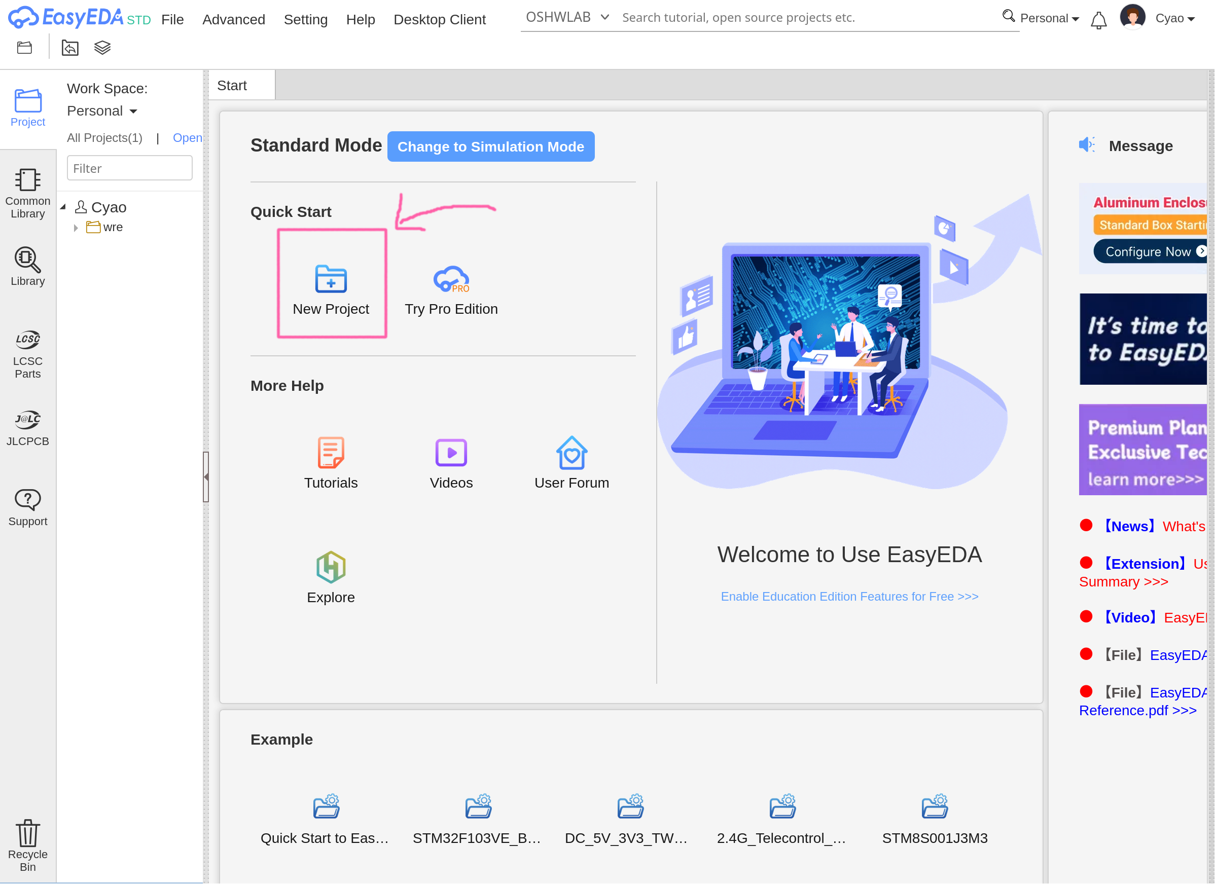
For making three button controlled LEDs, we need to add our parts in! In EasyEDA, go open the Common Library on the left side, find a resistor, and click on the triangle on it’s bottom right. Select “R-Axial-0.6” and place two of them!
Repeat this for adding a two LEDs, this time selecting “LED-TH-5mm”. Press R to rotate items. If you want to add buttons, select “K4-6×6_TH” in the switch/key part. And for the transistors, find the transistor symbol and select one of the TO92 options from the drop down menu.
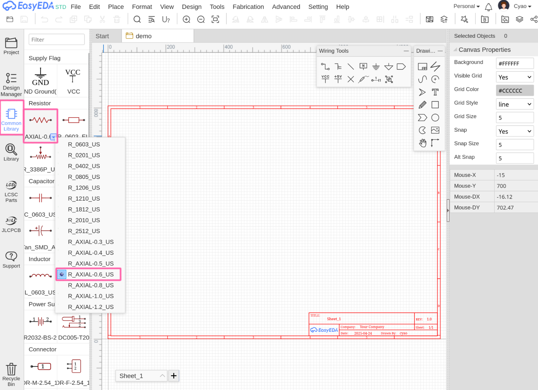
Now we need to add our battery holder: Click on the Library button on the left hand side, select LCSC and then search for C964834. Now click place.
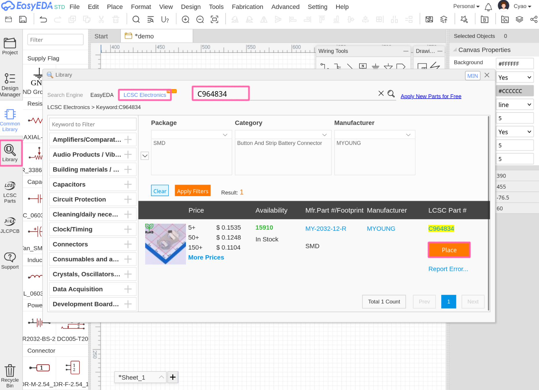
Your schematic should look something like this when you’re done!
We’re using CR2032s as batteries, which are 3V! So, on the + side of the terminal (Side with 1 written on it), it will be 3V, and on the opposite side, it will be ground.
When connected to the battery, the LEDs (called Light Emitting Diodes) will emmit light! The use of resistors is essential - they prevent too much electricity from passing through the LEDs. Without a resistor, the hungry LEDs would gobble up as much electricity as possible, and end up too hot and burn itself. (No, there won’t be any fires, they just make a small pop and turn black.) The resistors we’re using are 220ohms!
Time to add wires! Wires are basically paths that electricity will flow through. We would like to wire the positive end of our battery (the end where there is a +: Where electricity departs) up to the back of the LEDs. Then at the we wire the output of our LEDs up to the resistors. (You can change the order of the LED and resistor!) After that we will want to wire the other end of the reistor to the ground of the battery.
To do this, hover your mouse over one end of a symbol, press W and click on it to start wiring. Drag the wire around and wire your parts together. You should have something like this:
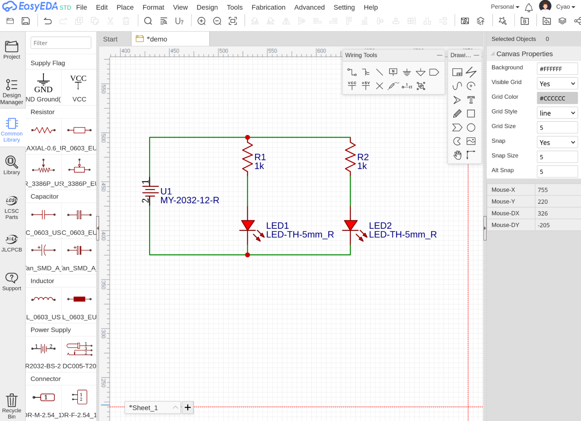
Save the schematic - you’re done with it! Now, onto the PCB!
Making the PCB
Now and press this button to convert your schematic to a PCB:
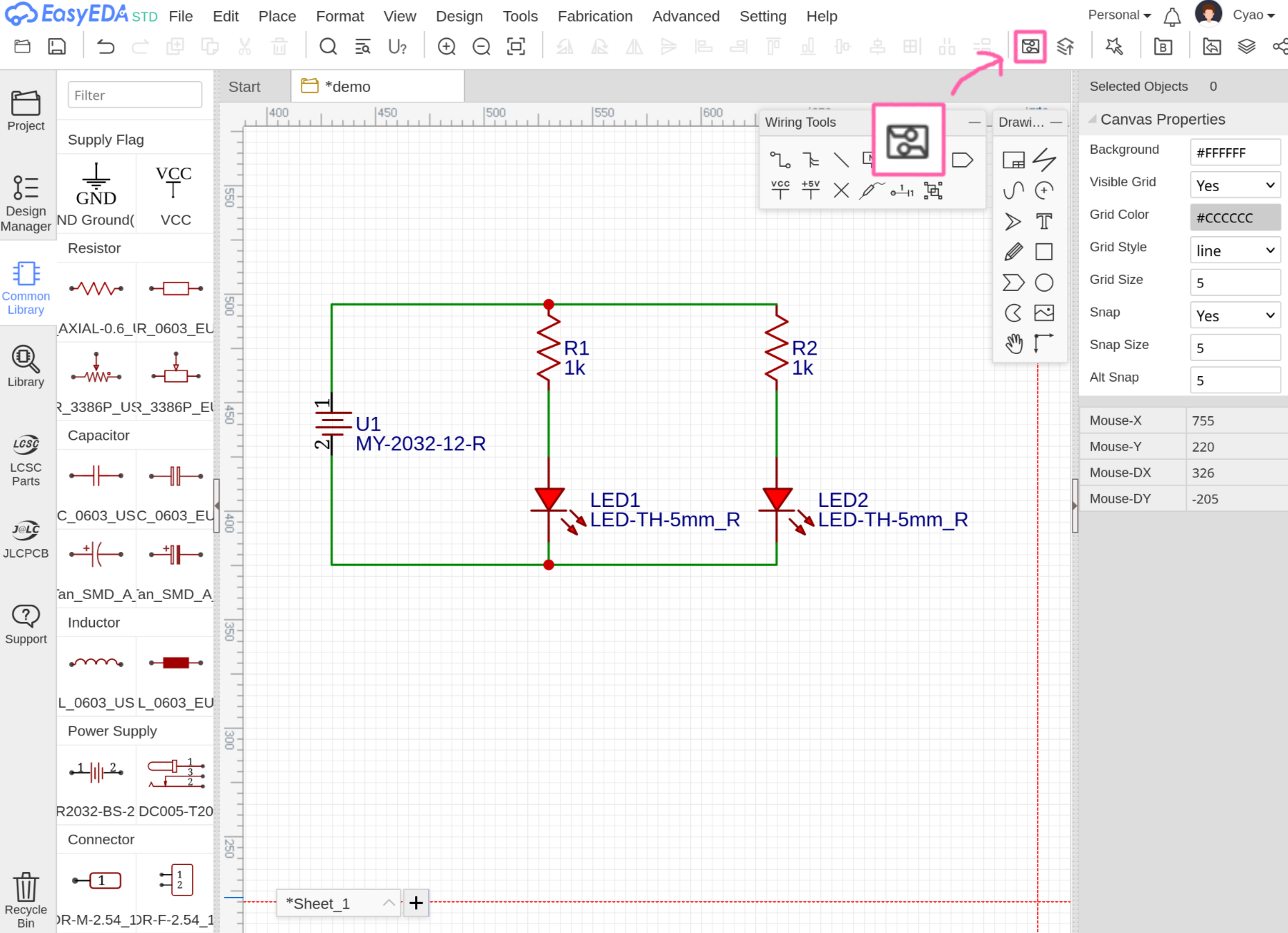
This PCB is a design of your IRL circuit board, so this time the placement of components will matter - where you place them is where they turn out on the final product, so think carefully where they should go!
Click on a component and you can drag them around, you can also press R to rotate. If you want to place a component on the back side, you can change it’s layer on the top right. Here is the placement I’m going with:
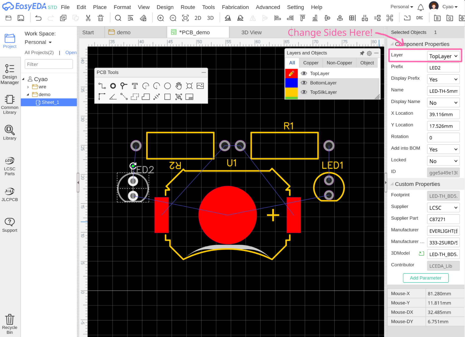
Remember to not block where the battery slides in with parts!
You should see a violet rectangle, click on it and press delete.
Now, go on the floating layers and objects menu, and select “BoardOutLine”. This is the outline of your board! Press W and you can draw an outline for your board. I’m going for a cat-like shape!
I highly recommend drawing a more detailed SVG (ie: Figma), export it as DXF then import it in by File > Import > Graphics and select mm as units, then “BoardOutLine” as the layer.
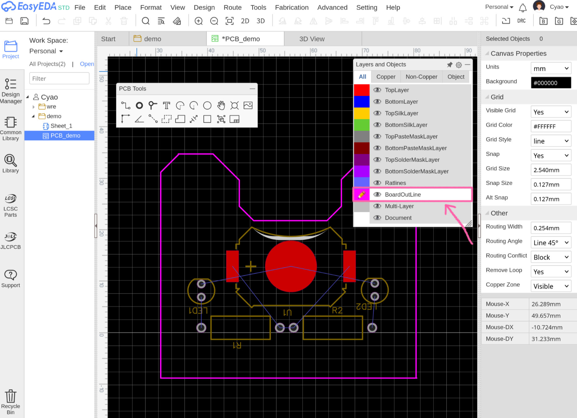
Great job! The only thing left is wiring the board. Switch back to the TopLayer on the layers and objects menu, click W to enter wireing mode, then click on any component pad. It and show you which direction you need to go with a thin white line:
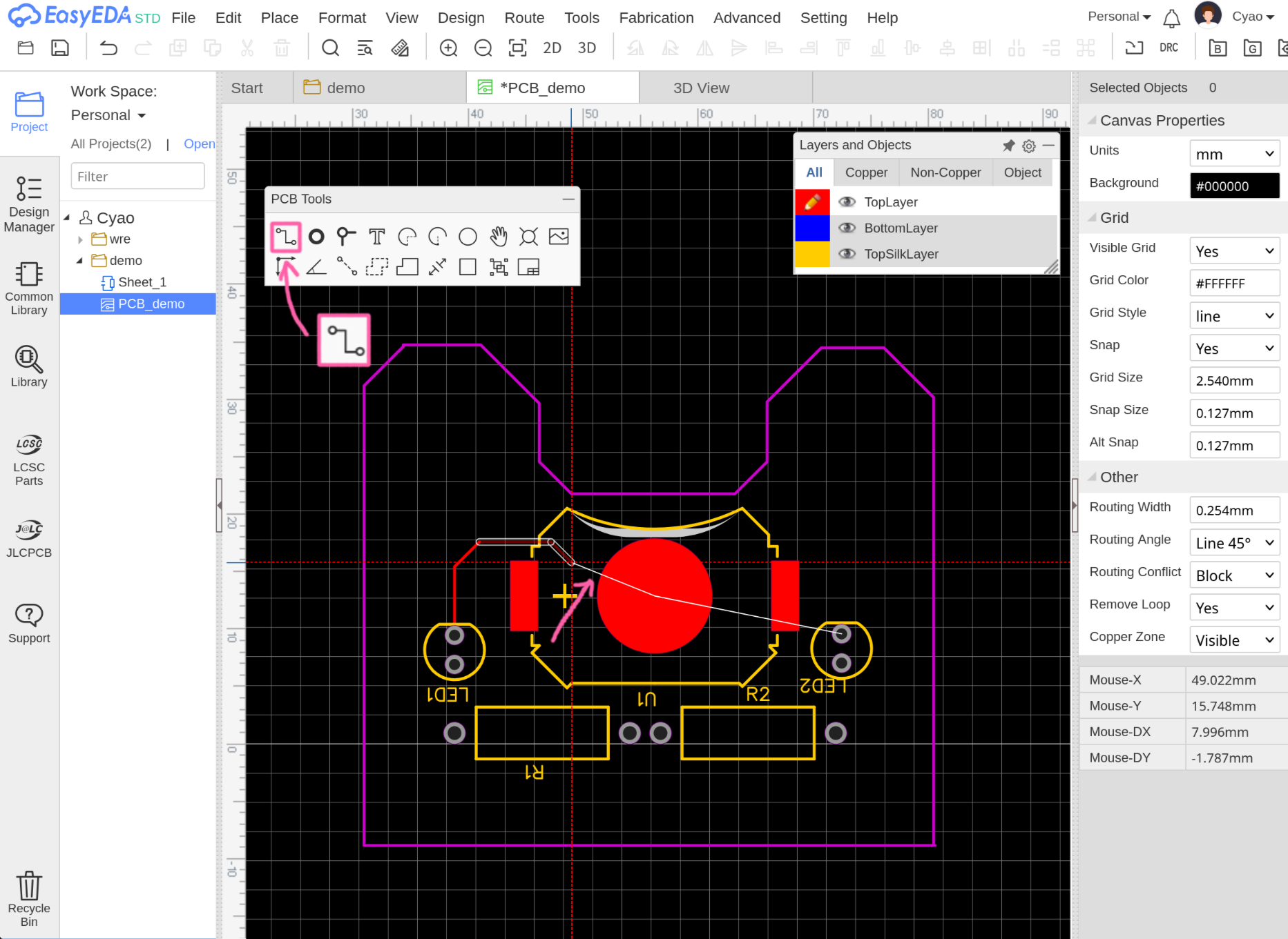
Attention! Wires and pads of different colors (except gray) can’t be connected together directly! You must via to the other side by pressing V and adding a via.
If you want to start routing from the back side, select “BottomLayer” on the layers and options menu.
Continue until there are no thin white lines (called ratlines) on the screen! Because my design is simple, I only need to wire on one side. The final product should look something like this:
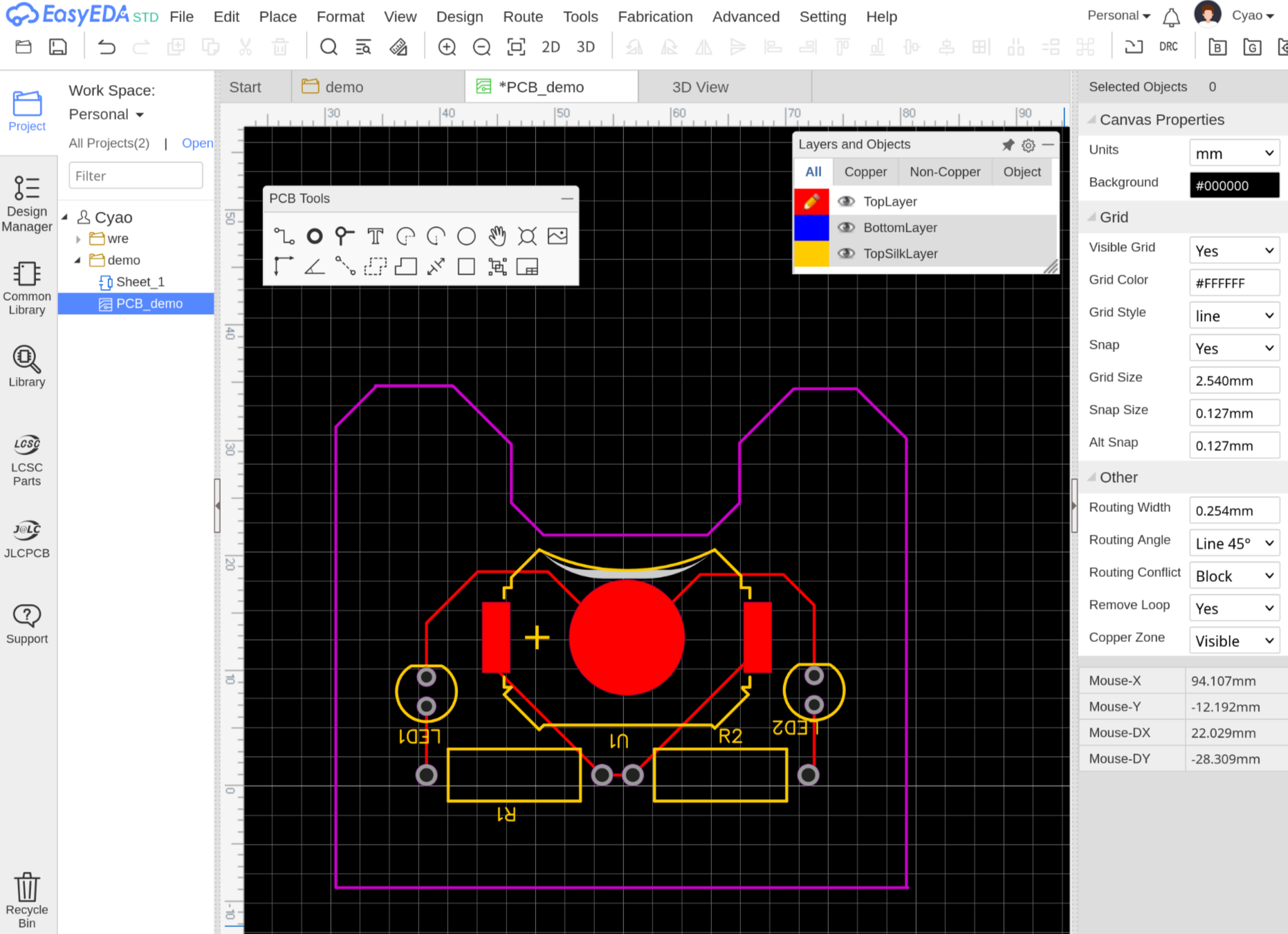
Good work! You’re almost done with the PCB. Let’s run the DRC to make sure the PCB works. Press the DRC button on the top right to run it and the results will be on the left side. Make sure there are no more errors!
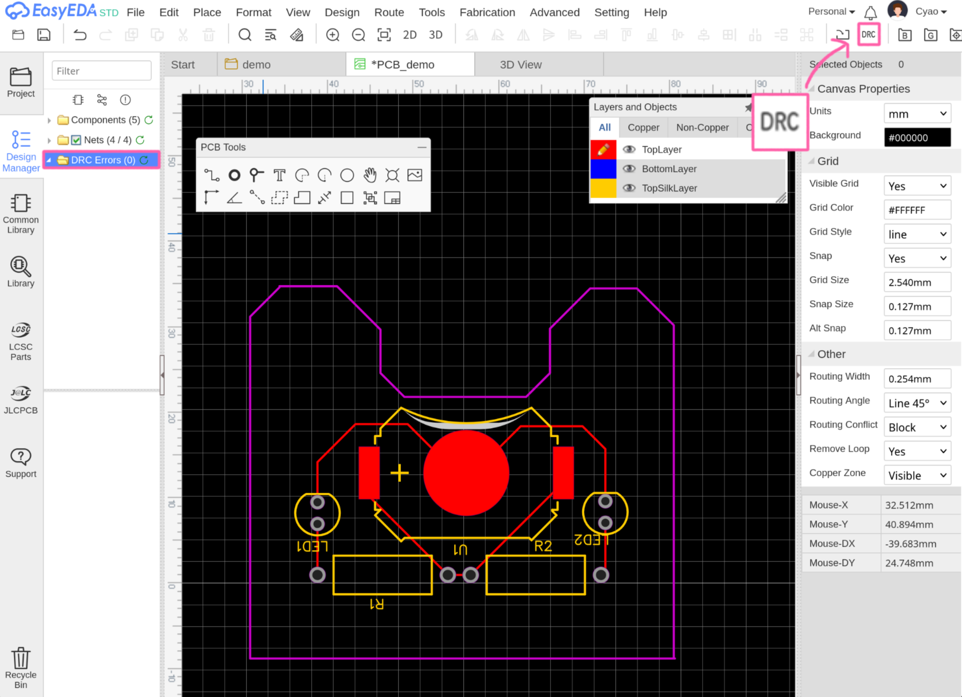
If there are, please resolve them! Otherwise, it’s time to pretty up the PCB! With the Text button (Or press S) on the pcb tools menu you can add some text to the PCB:
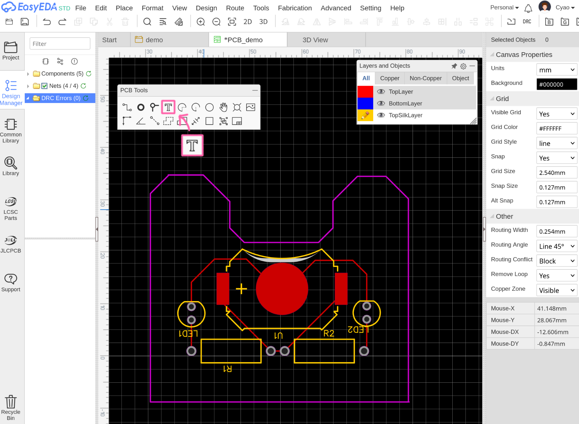
Be sure to select the layer “TopSilkScreen” beforhand! After that, it’s time for some graphics. Grab a picture on google or draw one yourself, then open up File > Import > Image. Load a source image, and drag the sliders tweak the output.
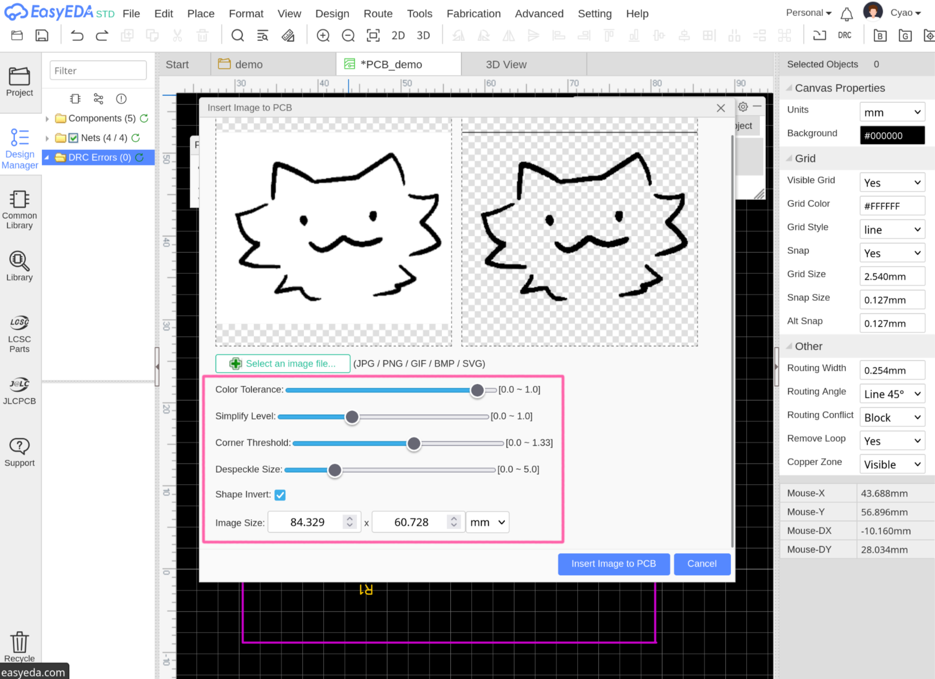
When your satisfied, click insert image to PCB. Now look at the beatiful drawing you have on your PCB!
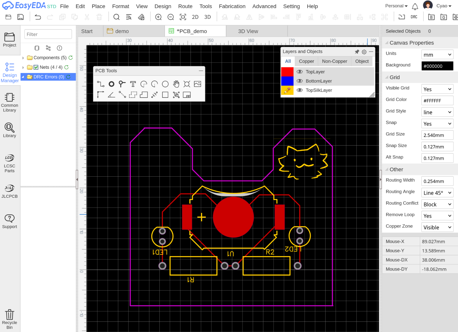
If it’s too big or too little, press M and use the ruler tool to measure the desired size. Now go back to the converter window, then change the output size to the measured size in the importer.
Lastly, we only need to generate the final fabrication file! Select Fabrication > One-click order PCB, and then press generate gerber. You will get a .zip file, that’s your fabrication file! (Don’t unzip it!)
Contgrats on making a PCB! You should find a .zip of your project in the “production” subfolder of your project’s directory - thats the file that you need to send to the manufaturers! All that’s left is to ship your project :D
Make a Github repo, and add all your files in!
One last step before submission - please take a screenshot of your schematic, PCB, and 3D view (Press Control+3), then put it inside your README.md of your project! (Create a README if you don’t have one.)
Now, head on to the How to Submit to go through the submission flow!